- 您现在的位置:买卖IC网 > Sheet目录138 > NSVBAT54LT1G (ON Semiconductor)DIODE SCHOTTKY 30V SOT-23-3
�  �
�
� � �  �
�
� � �  �
�
� � �  �
�
� � �  �
�
� � �  �
�
� � � BAT54LT1G, NSVBAT54LT1G�
� � http://onsemi.com�
� � 4�
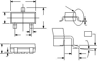
� � PACKAGE DIMENSIONS�
� � SOT?23 (TO?236)�
� � CASE 318?08�
� � ISSUE AP�
� � STYLE 8:�
� � PIN 1. ANODE�
� � 2. NO CONNECTION�
� � 3. CATHODE�
� � SCALE 10:1�
� � �
� � mm�
� � inches�
� � 0.8�
� � 0.031�
� � 0.9�
� � 0.035�
� � 0.95�
� � 0.037�
� � 0.95�
� � 0.037�
� � 2.0�
� � 0.079�
� � *For additional information on our Pb?Free strategy and soldering�
� � details, please download the ON Semiconductor Soldering and�
� � Mounting Techniques Reference Manual, SOLDERRM/D.�
� � SOLDERING FOOTPRINT*�
� � D�
� � A1�
� � 3�
� � 12�
� � NOTES:�
� � 1. DIMENSIONING AND TOLERANCING PER ANSI Y14.5M, 1982.�
� � 2. CONTROLLING DIMENSION: INCH.�
� � 3. MAXIMUM LEAD THICKNESS INCLUDES LEAD FINISH�
� � THICKNESS. MINIMUM LEAD THICKNESS IS THE MINIMUM�
� � THICKNESS OF BASE MATERIAL.�
� � 4. DIMENSIONS D AND E DO NOT INCLUDE MOLD FLASH,�
� � PROTRUSIONS, OR GATE BURRS.�
� � VIEW C�
� � L�
� � 0.25�
� � L1�
� � �
� � e�
� � E�
� � HE�
� � b�
� � A�
� � SEE VIEW C�
� � DIM�
� � A�
� � MIN NOM MAX MIN�
� � MILLIMETERS�
� � 0.89 1.00 1.11 0.035�
� � INCHES�
� � A1�
� � 0.01 0.06 0.10 0.001�
� � b�
� � 0.37 0.44 0.50 0.015�
� � c�
� � 0.09 0.13 0.18 0.003�
� � D�
� � 2.80 2.90 3.04 0.110�
� � E�
� � 1.20 1.30 1.40 0.047�
� � e�
� � 1.78 1.90 2.04 0.070�
� � L�
� � 0.10 0.20 0.30 0.004�
� � 0.040 0.044�
� � 0.002 0.004�
� � 0.018 0.020�
� � 0.005 0.007�
� � 0.114 0.120�
� � 0.051 0.055�
� � 0.075 0.081�
� � 0.008 0.012�
� � NOM MAX�
� � L1�
� � 2.10 2.40 2.64 0.083�
� � 0.094 0.104�
� � HE�
� � 0.35 0.54 0.69 0.014 0.021 0.029�
� � c�
� � 0°�
� � ???�
� � 10 0°�
� � °�
� � ???�
� � 10°�
� � �
� � ON Semiconductor�
� � and are registered trademarks of Semiconductor Co�
� � mponents Industries, LLC (SCILLC). SCILLC owns the rights to a number of patents, trademarks,�
� � copyrights, trade secrets, and other intellectual property. A listing of SCILLC’s product/patent coverage may be accessed at www.onsemi.com/site/pdf/Patent?Marking.pdf. SCILLC�
� � reserves the right to make changes without further notice to any products herein. SCILLC makes no warranty, representation or guarantee regarding the suitability of its products for any�
� � particular purpose, nor does SCILLC assume any liability arising out of the application or use of any product or circuit, and specifically disclaims any and all liability, including without�
� � limitation special, consequential or incidental damages. “Typical” parameters which may be provided in SCILLC data sheets and/or specifications can and do vary in different applications�
� � and actual performance may vary over time. All operating parameters, including “Typicals” must be validated for each customer application by customer’s technical experts. SCILLC�
� � does not convey any license under its patent rights nor the rights of others. SCILLC products are not designed, intended, or authorized for use as components in systems intended for�
� � surgical implant into the body, or other applications intended to support or sustain life, or for any other application in which the failure of the SCILLC product could create a situation where�
� � personal injury or death may occur. Should Buyer purchase or use SCILLC products for any such unintended or unauthorized application, Buyer shall indemnify and hold SCILLC and�
� � its officers, employees, subsidiaries, affiliates, and distributors harmless against all claims, costs, damages, and expenses, and reasonable attorney fees arising out of, directly or indirectly,�
� � any claim of personal injury or death associated with such unintended or unauthorized use, even if such claim alleges that SCILLC was negligent regarding the design or manufacture�
� � of the part. SCILLC is an Equal Opportunity/Affirmative Action Employer. This literature is subject to all applicable copyright laws and is not for resale in any manner.�
� � PUBLICATION ORDERING INFORMATION�
� � N. American Technical Support: 800?282?9855 Toll Free�
� � USA/Canada�
� � Europe, Middle East and Africa Technical Support:�
� � Phone: 421 33 790 2910�
� � Japan Customer Focus Center�
� � Phone: 81?3?5817?1050�
� � BAT54LT1/D�
� � LITERATURE FULFILLMENT:�
� � Literature Distribution Center for ON Semiconductor�
� � P.O. Box 5163, Denver, Colorado 80217 USA�
� � Phone: 303?675?2175 or 800?344?3860 Toll Free USA/Canada�
� � Fax: 303?675?2176 or 800?344?3867�
� � Toll Free USA/Canada�
� � Email: orderlit@onsemi.com�
� � ON Semiconductor Website: www.onsemi.com�
� � Order Literature: http://www.onsemi.com/orderlit�
� � For additional information, please contact your local�
� � Sales Representative�
� 发布紧急采购,3分钟左右您将得到回复。
相关PDF资料
NSVR0230M2T5G
DIODE SCHOTTKY 200MA 30V SOD723
NSVR0240V2T1G
DIODE SCHOTTKY 40V 250MA SOD523
NSVR0320MW2T1G
DIODE SCHOTTKY 1A 20V SOD-323
NSVRB521S30T1G
DIODE SCHOTTKY 200MA 30V SOD523
NTSB30100S-1G
DIODE LVFR 30A 100V I2PAK
NTST20100CTG
IC DIODE SCHOTTKY 100V TO220-3
NTST30100CTG
IC DIODE SCHOTTKY 100V TO220-3
NTST30U100CTG
IC DIODE SCHOTTKY 100V TO220-3
相关代理商/技术参数
NSVBAT54SWT1G
功能描述:肖特基二极管与整流器 SS SHKY DIO 30V TR RoHS:否 制造商:Skyworks Solutions, Inc. 产品:Schottky Diodes 峰值反向电压:2 V 正向连续电流:50 mA 最大浪涌电流: 配置:Crossover Quad 恢复时间: 正向电压下降:370 mV 最大反向漏泄电流: 最大功率耗散:75 mW 工作温度范围:- 65 C to + 150 C 安装风格:SMD/SMT 封装 / 箱体:SOT-143 封装:Reel
NSVBAT54WT1G
功能描述:肖特基二极管与整流器 SS SHKY DIO 30V TR RoHS:否 制造商:Skyworks Solutions, Inc. 产品:Schottky Diodes 峰值反向电压:2 V 正向连续电流:50 mA 最大浪涌电流: 配置:Crossover Quad 恢复时间: 正向电压下降:370 mV 最大反向漏泄电流: 最大功率耗散:75 mW 工作温度范围:- 65 C to + 150 C 安装风格:SMD/SMT 封装 / 箱体:SOT-143 封装:Reel
NSVBAV70TT1
制造商:Rochester Electronics LLC 功能描述:- Tape and Reel
NSVBAV70TT1G
功能描述:DIODE SWITCH DUAL 70V SC75-3 RoHS:是 类别:分离式半导体产品 >> 二极管,整流器 - 阵列 系列:- 其它有关文件:STTH10LCD06C View All Specifications 标准包装:1,000 系列:- 电压 - 在 If 时为正向 (Vf)(最大):2V @ 5A 电流 - 在 Vr 时反向漏电:1µA @ 600V 电流 - 平均整流 (Io)(每个二极管):5A 电压 - (Vr)(最大):600V 反向恢复时间(trr):50ns 二极管类型:标准 速度:快速恢复 = 200mA(Io) 二极管配置:1 对共阴极 安装类型:表面贴装 封装/外壳:TO-263-3,D²Pak(2 引线+接片),TO-263AB 供应商设备封装:D2PAK 包装:带卷 (TR) 产品目录页面:1553 (CN2011-ZH PDF) 其它名称:497-10107-2
NSVBAV70TT3G
功能描述:二极管 - 通用,功率,开关 DUAL SWITCHING DIODE RoHS:否 制造商:STMicroelectronics 产品:Switching Diodes 峰值反向电压:600 V 正向连续电流:200 A 最大浪涌电流:800 A 配置: 恢复时间:2000 ns 正向电压下降:1.25 V 最大反向漏泄电流:300 uA 最大功率耗散: 工作温度范围: 安装风格:SMD/SMT 封装 / 箱体:ISOTOP 封装:Tube
NSVBC114YDXV6T1G
功能描述:两极晶体管 - BJT SS RSTR XSTR TR RoHS:否 制造商:STMicroelectronics 配置: 晶体管极性:PNP 集电极—基极电压 VCBO: 集电极—发射极最大电压 VCEO:- 40 V 发射极 - 基极电压 VEBO:- 6 V 集电极—射极饱和电压: 最大直流电集电极电流: 增益带宽产品fT: 直流集电极/Base Gain hfe Min:100 A 最大工作温度: 安装风格:SMD/SMT 封装 / 箱体:PowerFLAT 2 x 2
NSVBC114YPDXV65G
功能描述:TRANSISTOR BRT DUAL NPN SOT-563 RoHS:是 类别:分离式半导体产品 >> 晶体管(BJT) - 阵列﹐预偏压式 系列:- 标准包装:3,000 系列:- 晶体管类型:1 个 NPN,1 个 PNP - 预偏压式(双) 电流 - 集电极 (Ic)(最大):70mA,100mA 电压 - 集电极发射极击穿(最大):50V 电阻器 - 基极 (R1)(欧):47k,2.2k 电阻器 - 发射极 (R2)(欧):47k 在某 Ic、Vce 时的最小直流电流增益 (hFE):70 @ 5mA,5V Ib、Ic条件下的Vce饱和度(最大):300mV @ 500µA,10mA 电流 - 集电极截止(最大):- 频率 - 转换:100MHz,200MHz 功率 - 最大:250mW 安装类型:表面贴装 封装/外壳:6-TSSOP,SC-88,SOT-363 供应商设备封装:PG-SOT363-6 包装:带卷 (TR) 其它名称:SP000784046
NSVBC124EDXV6T1G
制造商:ON Semiconductor 功能描述:SS SOT563 DUAL RSTR XSTR - Tape and Reel